6
RF Device Data
Freescale Semiconductor
MRF6S27085HR3 MRF6S27085HSR3
TYPICAL CHARACTERISTICS
?70
?30
?40
?45
?50
?60
?35
?55
?65
Figure 7. Intermodulation Distortion Products
versus Tone Spacing
1 10010
?60
0
0.1
7th Order
TWO?TONE SPACING (MHz)
VDD
= 28 Vdc, P
out
= 85 W (PEP), I
DQ
= 900 mA
Two?Tone Measurements
(f1 + f2)/2 = Center Frequency of 2645 MHz
5th Order
3rd Order
?10
?20
?30
?40
?50
Figure 8. Pulsed CW Output Power versus
Input Power
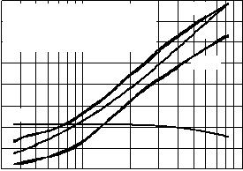
Figure 9. Single-Carrier N-CDMA ACPR, ALT1,
Power Gain and Drain Efficiency versus Output
Power
5
Pout, OUTPUT POWER (WATTS) AVG. W?CDMA
45
35
30
10
10 100
20
40
56
31
Pin, INPUT POWER (dBm)
54
52
50
46
32 3433 3635 3937
38
55
51
53
49
30
0
20
5
45
Pout, OUTPUT POWER (WATTS) CW
Figure 10. Power Gain and Drain Efficiency
versus CW Output Power
VDD
= 28 Vdc, I
DQ
= 900 mA
f = 2645 MHz
10
17.5
15
10
5
2.5
40
30
25
20
15
10
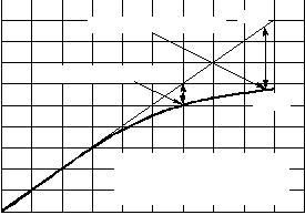
Figure 11. Power Gain versus Output Power
Pout, OUTPUT POWER (WATTS) CW
VDD
= 24 V
ACPR
η
D
, DRAIN EFFICIENCY (%), G
ps
, POWER GAIN (dB)
IMD, INTERMODULATION DISTORTION (dBc)
ACPR (dBc), ALT1 (dBc)
η
D
,
DRAIN EFFICIENCY (%)
ηD
G
ps
, POWER GAIN (dB)
11
16
1 10010
13
12
15
14
IDQ
= 900 mA
f = 2645 MHz
P
out
, OUTPUT POWER (dBm)
G
ps
, POWER GAIN (dB)
48
47
ηD
100
32 V
Actual
Ideal
P1dB = 51 dBm (126.74 W)
P3dB = 51.72 dBm (148.54 W)
40
25
15
VDD= 28 Vdc, IDQ
= 900 mA, f = 2645 MHz
Single?Carrier N?CDMA, 1.2288 MHz
Channel Bandwidth, PAR = 9.8 dB
@ 0.01% Probability (CCDF)
ALT1
12.5
7.5
35
28 V
Gps
Gps
VDD
= 28 Vdc, I
DQ
= 900 mA
Pulsed CW, 8 μsec(on), 1 msec(off)
f = 2645 MHz


发布紧急采购,3分钟左右您将得到回复。
相关PDF资料
MRF6S9045NR1
MOSFET RF N-CH 28V 10W TO-270-2
MRF6S9060NR1
MOSFET RF N-CH 28V 14W TO-270-2
MRF6S9125MR1
MOSFET RF N-CH 28V 27W TO-270-4
MRF6S9125NR1
MOSFET RF N-CH 28V 27W TO-270-4
MRF6S9130HSR5
MOSFET RF N-CHAN 28V 27W NI-780S
MRF6S9160HSR5
MOSFET RF N-CHAN 28V 35W NI-780S
MRF6V10010NR4
MOSFET RF N-CHAN PLD-1.5
MRF6V10250HSR5
MOSFET RF N-CH NI780S
相关代理商/技术参数
MRF6S9045
制造商:FREESCALE 制造商全称:Freescale Semiconductor, Inc 功能描述:RF Power Field Effect Transistors
MRF6S9045MBR1
功能描述:MOSFET RF N-CH 28V 10W TO-272-2 RoHS:否 类别:分离式半导体产品 >> RF FET 系列:- 产品目录绘图:MOSFET SOT-23-3 Pkg 标准包装:3,000 系列:- 晶体管类型:N 通道 JFET 频率:- 增益:- 电压 - 测试:- 额定电流:30mA 噪音数据:- 电流 - 测试:- 功率 - 输出:- 电压 - 额定:25V 封装/外壳:TO-236-3,SC-59,SOT-23-3 供应商设备封装:SOT-23-3(TO-236) 包装:带卷 (TR) 产品目录页面:1558 (CN2011-ZH PDF) 其它名称:MMBFJ309LT1GOSMMBFJ309LT1GOS-NDMMBFJ309LT1GOSTR
MRF6S9045MR1
功能描述:MOSFET RF N-CH 28V 10W TO-270-2 RoHS:是 类别:分离式半导体产品 >> RF FET 系列:- 产品目录绘图:MOSFET SOT-23-3 Pkg 标准包装:3,000 系列:- 晶体管类型:N 通道 JFET 频率:- 增益:- 电压 - 测试:- 额定电流:30mA 噪音数据:- 电流 - 测试:- 功率 - 输出:- 电压 - 额定:25V 封装/外壳:TO-236-3,SC-59,SOT-23-3 供应商设备封装:SOT-23-3(TO-236) 包装:带卷 (TR) 产品目录页面:1558 (CN2011-ZH PDF) 其它名称:MMBFJ309LT1GOSMMBFJ309LT1GOS-NDMMBFJ309LT1GOSTR
MRF6S9045N
制造商:FREESCALE 制造商全称:Freescale Semiconductor, Inc 功能描述:RF Power Field Effect Transistors
MRF6S9045NBR1
功能描述:MOSFET RF N-CH 28V 10W TO-272-2 RoHS:是 类别:分离式半导体产品 >> RF FET 系列:- 产品目录绘图:MOSFET SOT-23-3 Pkg 标准包装:3,000 系列:- 晶体管类型:N 通道 JFET 频率:- 增益:- 电压 - 测试:- 额定电流:30mA 噪音数据:- 电流 - 测试:- 功率 - 输出:- 电压 - 额定:25V 封装/外壳:TO-236-3,SC-59,SOT-23-3 供应商设备封装:SOT-23-3(TO-236) 包装:带卷 (TR) 产品目录页面:1558 (CN2011-ZH PDF) 其它名称:MMBFJ309LT1GOSMMBFJ309LT1GOS-NDMMBFJ309LT1GOSTR
MRF6S9045NR1
功能描述:MOSFET RF N-CH 28V 10W TO-270-2 RoHS:是 类别:分离式半导体产品 >> RF FET 系列:- 产品目录绘图:MOSFET SOT-23-3 Pkg 标准包装:3,000 系列:- 晶体管类型:N 通道 JFET 频率:- 增益:- 电压 - 测试:- 额定电流:30mA 噪音数据:- 电流 - 测试:- 功率 - 输出:- 电压 - 额定:25V 封装/外壳:TO-236-3,SC-59,SOT-23-3 供应商设备封装:SOT-23-3(TO-236) 包装:带卷 (TR) 产品目录页面:1558 (CN2011-ZH PDF) 其它名称:MMBFJ309LT1GOSMMBFJ309LT1GOS-NDMMBFJ309LT1GOSTR
MRF6S9045NR1_08
制造商:FREESCALE 制造商全称:Freescale Semiconductor, Inc 功能描述:RF Power Field Effect Transistors N-Channel Enhancement-Mode Lateral MOSFETs
MRF6S9060
制造商:FREESCALE 制造商全称:Freescale Semiconductor, Inc 功能描述:RF Power Field Effect Transistors
